Conditions for the occurrence of current in a semiconductor. Electric current in semiconductors. semiconductor diode. Semiconductor devices. Electric Current in Vacuum
In this lesson, we will consider such a medium for the passage of electric current as semiconductors. We will consider the principle of their conductivity, the dependence of this conductivity on temperature and the presence of impurities, consider such a concept as p-n junction and basic semiconductor devices.
If you make a direct connection, then the external field will neutralize the locking one, and the current will be made by the main charge carriers (Fig. 9).


Rice. 9. p-n junction with direct connection ()
In this case, the current of minority carriers is negligible, it is practically non-existent. Therefore, the p-n junction provides one-way conduction of electric current.

Rice. 10. Atomic structure of silicon with increasing temperature
The conduction of semiconductors is electron-hole, and such conduction is called intrinsic conduction. And unlike conductive metals, as the temperature increases, the number of free charges just increases (in the first case, it does not change), so the conductivity of semiconductors increases with increasing temperature, and the resistance decreases (Fig. 10).
A very important issue in the study of semiconductors is the presence of impurities in them. And in the case of the presence of impurities, one should speak of impurity conductivity.
Semiconductors
The small size and very high quality of transmitted signals have made semiconductor devices very common in modern electronic technology. The composition of such devices can include not only the aforementioned silicon with impurities, but also, for example, germanium.
One of these devices is a diode - a device capable of passing current in one direction and preventing its passage in the other. It is obtained by implanting another type of semiconductor into a p- or n-type semiconductor crystal (Fig. 11).

Rice. 11. The designation of the diode on the diagram and the diagram of its device, respectively
Another device, now with two p-n junctions, is called a transistor. It serves not only to select the direction of current flow, but also to convert it (Fig. 12).
Rice. 12. Scheme of the structure of the transistor and its designation on the electrical circuit, respectively ()
It should be noted that modern microcircuits use many combinations of diodes, transistors and other electrical devices.
In the next lesson, we will look at the propagation of electric current in a vacuum.
Bibliography
- Tikhomirova S.A., Yavorsky B.M. Physics (basic level) - M.: Mnemozina, 2012.
- Gendenstein L.E., Dick Yu.I. Physics grade 10. - M.: Ileksa, 2005.
- Myakishev G.Ya., Sinyakov A.Z., Slobodskov B.A. Physics. Electrodynamics. - M.: 2010.
- Principles of operation of devices ().
- Encyclopedia of Physics and Technology ().
Homework
- What causes conduction electrons in a semiconductor?
- What is intrinsic conductivity of a semiconductor?
- How does the conductivity of a semiconductor depend on temperature?
- What is the difference between a donor impurity and an acceptor impurity?
- * What is the conductivity of silicon with an admixture of a) gallium, b) indium, c) phosphorus, d) antimony?
Semiconductors are substances that occupy an intermediate position in terms of electrical conductivity between good conductors and good insulators (dielectrics).
Semiconductors are also chemical elements (germanium Ge, silicon Si, selenium Se, tellurium Te), and compounds of chemical elements (PbS, CdS, etc.).
The nature of current carriers in different semiconductors is different. In some of them, charge carriers are ions; in others, the charge carriers are electrons.
Intrinsic conductivity of semiconductors
There are two types of intrinsic conduction in semiconductors: electronic conduction and hole conduction in semiconductors.
1. Electronic conductivity of semiconductors.
Electronic conductivity is carried out by directed movement in the interatomic space of free electrons that have left the valence shell of the atom as a result of external influences.
2. Hole conductivity of semiconductors.
Hole conduction is carried out with the directed movement of valence electrons to vacant places in pair-electron bonds - holes. The valence electron of a neutral atom located in close proximity to a positive ion (hole) is attracted to the hole and jumps into it. In this case, a positive ion (hole) is formed in place of a neutral atom, and a neutral atom is formed in place of a positive ion (hole).

In an ideally pure semiconductor without any foreign impurities, each free electron corresponds to the formation of one hole, i.e. the number of electrons and holes involved in the creation of the current is the same.
The conductivity at which the same number of charge carriers (electrons and holes) occurs is called the intrinsic conductivity of semiconductors.
The intrinsic conductivity of semiconductors is usually small, since the number of free electrons is small. The slightest traces of impurities radically change the properties of semiconductors.
Electrical conductivity of semiconductors in the presence of impurities
Impurities in a semiconductor are atoms of foreign chemical elements that are not contained in the main semiconductor.
Impurity conductivity- this is the conductivity of semiconductors, due to the introduction of impurities into their crystal lattices.
In some cases, the influence of impurities manifests itself in the fact that the "hole" mechanism of conduction becomes practically impossible, and the current in the semiconductor is carried out mainly by the movement of free electrons. Such semiconductors are called electronic semiconductors or n-type semiconductors(from the Latin word negativus - negative). The main charge carriers are electrons, and not the main ones are holes. n-type semiconductors are semiconductors with donor impurities.
1. Donor impurities.
Donor impurities are those that easily donate electrons and, consequently, increase the number of free electrons. Donor impurities supply conduction electrons without the appearance of the same number of holes.
 A typical example of a donor impurity in tetravalent germanium Ge are pentavalent arsenic atoms As.
In other cases, the movement of free electrons becomes practically impossible, and the current is carried out only by the movement of holes. These semiconductors are called hole semiconductors or p-type semiconductors(from the Latin word positivus - positive). The main charge carriers are holes, and not the main - electrons. . Semiconductors of the p-type are semiconductors with acceptor impurities.
Acceptor impurities are impurities in which there are not enough electrons to form normal pair-electron bonds.
An example of an acceptor impurity in germanium Ge are trivalent gallium atoms Ga

Electric current through the contact of semiconductors of p-type and n-type p-n junction is the contact layer of two impurity semiconductors of p-type and n-type; The p-n junction is a boundary separating regions with hole (p) conduction and electronic (n) conduction in the same single crystal.
direct p-n junction
If the n-semiconductor is connected to the negative pole of the power source, and the positive pole of the power source is connected to the p-semiconductor, then under the action of an electric field, the electrons in the n-semiconductor and the holes in the p-semiconductor will move towards each other to the semiconductor interface. Electrons, crossing the boundary, "fill" the holes, the current through the pn junction is carried out by the main charge carriers. As a result, the conductivity of the entire sample increases. With such a direct (throughput) direction of the external electric field, the thickness of the barrier layer and its resistance decrease.
In this direction, the current passes through the boundary of the two semiconductors.
  |
Reverse pn junction
If the n-semiconductor is connected to the positive pole of the power source, and the p-semiconductor is connected to the negative pole of the power source, then the electrons in the n-semiconductor and holes in the p-semiconductor under the action of an electric field will move from the interface in opposite directions, the current through p -n-transition is carried out by minor charge carriers. This leads to a thickening of the barrier layer and an increase in its resistance. As a result, the conductivity of the sample turns out to be insignificant, and the resistance is large.
A so-called barrier layer is formed. With this direction of the external field, the electric current practically does not pass through the contact of the p- and n-semiconductors.


Thus, the electron-hole transition has one-sided conduction.
The dependence of the current on the voltage - volt - current characteristic of the p-n junction is shown in the figure (volt - current characteristic of the direct p-n junction is shown by a solid line, volt - ampere characteristic of the reverse p-n junction is shown by a dotted line).

Semiconductors:
Semiconductor diode - for rectifying alternating current, it uses one p - n - junction with different resistances: in the forward direction, the resistance of the p - n - junction is much less than in the reverse direction.
Photoresistors - for registration and measurement of weak light fluxes. With their help, determine the quality of surfaces, control the dimensions of products.
Thermistors - for remote temperature measurement, fire alarms.
Semiconductors are a class of substances in which, with increasing temperature, conductivity increases and electrical resistance decreases. This semiconductors are fundamentally different from metals.
Typical semiconductors are crystals of germanium and silicon, in which the atoms are united by a covalent bond. Semiconductors have free electrons at any temperature. Free electrons under the action of an external electric field can move in the crystal, creating an electronic conduction current. The removal of an electron from the outer shell of one of the atoms of the crystal lattice leads to the transformation of this atom into a positive ion. This ion can be neutralized by capturing an electron from one of the neighboring atoms. Further, as a result of the transitions of electrons from atoms to positive ions, a process of chaotic movement in the crystal of the place with the missing electron occurs. Externally, this process is perceived as the movement of a positive electric charge, called hole.
When a crystal is placed in an electric field, an ordered motion of holes occurs - a hole conduction current.
In an ideal semiconductor crystal, an electric current is created by the movement of an equal number of negatively charged electrons and positively charged holes. Conductivity in ideal semiconductors is called intrinsic conductivity.
The properties of semiconductors are highly dependent on the content of impurities. Impurities are of two types - donor and acceptor.
Impurities that donate electrons and create electronic conductivity are called donor(impurities having a valence greater than that of the main semiconductor). Semiconductors in which the concentration of electrons exceeds the concentration of holes are called n-type semiconductors.
Impurities that capture electrons and thereby create mobile holes without increasing the number of conduction electrons are called acceptor(impurities having a valence less than that of the main semiconductor).
At low temperatures, holes are the main current carriers in a semiconductor crystal with an acceptor impurity, and electrons are not the main carriers. Semiconductors in which the concentration of holes exceeds the concentration of conduction electrons are called hole semiconductors or p-type semiconductors. Consider the contact of two semiconductors with different types of conductivity.
Mutual diffusion of the majority carriers occurs through the boundary of these semiconductors: electrons diffuse from the n-semiconductor into the p-semiconductor, and holes from the p-semiconductor into the n-semiconductor. As a result, the section of the n-semiconductor adjacent to the contact will be depleted in electrons, and an excess positive charge will form in it, due to the presence of bare impurity ions. The movement of holes from the p-semiconductor to the n-semiconductor leads to the appearance of an excess negative charge in the boundary region of the p-semiconductor. As a result, a double electric layer is formed, and a contact electric field arises, which prevents further diffusion of the main charge carriers. This layer is called locking.
An external electric field affects the electrical conductivity of the barrier layer. If the semiconductors are connected to the source as shown in Fig. 55, then under the action of an external electric field, the main charge carriers - free electrons in the n-semiconductor and holes in the p-semiconductor - will move towards each other to the interface of the semiconductors, while the thickness of the p-n junction decreases, therefore, its resistance decreases. In this case, the current strength is limited by external resistance. This direction of the external electric field is called direct. The direct connection of the p-n-junction corresponds to section 1 on the current-voltage characteristic (see Fig. 57).
Electric current carriers in various media and current-voltage characteristics are summarized in Table. one.
If the semiconductors are connected to the source as shown in Fig. 56, then the electrons in the n-semiconductor and the holes in the p-semiconductor will move under the action of an external electric field from the boundary in opposite directions. The thickness of the barrier layer and hence its resistance increase. With this direction of the external electric field - the reverse (blocking) only minor charge carriers pass through the interface, the concentration of which is much less than the main ones, and the current is practically zero. The reverse inclusion of the pn junction corresponds to section 2 on the current-voltage characteristic (Fig. 57).
Thus, the p-n junction has an asymmetric conductivity. This property is used in semiconductor diodes containing a single p-n junction and used, for example, for AC rectification or detection.

Semiconductors are widely used in modern electronic technology.
The dependence of the electrical resistance of semiconductor metals on temperature is used in special semiconductor devices - thermistors. Devices that use the property of semiconductor crystals to change their electrical resistance when illuminated by light are called photoresistors.
Electric Current in Vacuum
If two electrodes are placed in a sealed vessel and air is removed from the vessel, then an electric current does not arise in a vacuum - there are no electric current carriers. The American scientist T. A. Edison (1847-1931) discovered in 1879 that an electric current can occur in a vacuum glass flask if one of the electrodes in it is heated to a high temperature. The phenomenon of emission of free electrons from the surface of heated bodies is called thermionic emission. The work that must be done to release an electron from the surface of the body is called the work function. The phenomenon of thermionic emission is explained by the fact that with an increase in body temperature, the kinetic energy of a certain part of the electrons in the substance increases. If the kinetic energy of an electron exceeds the work function, then it can overcome the action of attractive forces from positive ions and leave the surface of the body in a vacuum. The operation of various electron tubes is based on the phenomenon of thermionic emission.
Semiconductor- this is a substance in which the resistivity can vary over a wide range and decreases very quickly with increasing temperature, which means that the electrical conductivity (1 / R) increases.
- observed in silicon, germanium, selenium and in some compounds.
Conduction mechanism semiconductors
Semiconductor crystals have an atomic crystal lattice, where outer electrons are bound to neighboring atoms by covalent bonds.
At low temperatures, pure semiconductors have no free electrons and it behaves like a dielectric.
Semiconductors are pure (no impurities)
If the semiconductor is pure (without impurities), then it has own conductivity, which is small.
There are two types of intrinsic conduction:
1 electronic(conductivity "n" - type)
At low temperatures in semiconductors, all electrons are associated with nuclei and the resistance is large; as the temperature increases, the kinetic energy of the particles increases, the bonds break and free electrons appear - the resistance decreases.
Free electrons move opposite to the electric field strength vector.
The electronic conductivity of semiconductors is due to the presence of free electrons.
2. perforated(conductivity "p"-type)
With an increase in temperature, the covalent bonds between atoms are destroyed, carried out by valence electrons, and places with a missing electron are formed - a "hole".
It can move throughout the crystal, because. its place can be replaced by valence electrons. Moving a "hole" is equivalent to moving a positive charge.
The hole moves in the direction of the electric field strength vector.
In addition to heating, the breaking of covalent bonds and the appearance of intrinsic conductivity of semiconductors can be caused by illumination (photoconductivity) and the action of strong electric fields.


The total conductivity of a pure semiconductor is the sum of the conductivities of the "p" and "n" types
and is called electron-hole conductivity.
Semiconductors in the presence of impurities
They have own + impurity conductivity
The presence of impurities greatly increases the conductivity.
When the concentration of impurities changes, the number of carriers of the electric current - electrons and holes - changes.
The ability to control the current underlies the widespread use of semiconductors.
Exist:
1)donor impurities (giving off)
They are additional suppliers of electrons to semiconductor crystals, easily donate electrons and increase the number of free electrons in a semiconductor.
These are conductors "n" - type, i.e. semiconductors with donor impurities, where the main charge carrier is electrons, and the minority is holes.
Such a semiconductor has electronic impurity conductivity.

For example, arsenic.
2. acceptor impurities (host)
They create "holes" by taking electrons into themselves.
These are semiconductors "p" - type, those. semiconductors with acceptor impurities, where the main charge carrier is holes, and the minority is electrons.
Such a semiconductor has hole impurity conductivity.

For example, indium.
Electrical properties of "p-n" junction
"p-n" transition(or electron-hole transition) - the contact area of two semiconductors, where the conductivity changes from electronic to hole (or vice versa).
In a semiconductor crystal, such regions can be created by introducing impurities. In the contact zone of two semiconductors with different conductivities, mutual diffusion will take place. electrons and holes and a blocking electric layer is formed. The electric field of the blocking layer prevents the further transition of electrons and holes through the boundary. The barrier layer has an increased resistance compared to other areas of the semiconductor.
 The external electric field affects the resistance of the barrier layer.
 With the direct (transmission) direction of the external electric field, the electric current passes through the boundary of two semiconductors.
Because electrons and holes move towards each other to the interface, then the electrons, crossing the interface, fill the holes. The thickness of the barrier layer and its resistance are continuously decreasing.
Access mode p-n transition:

With the blocking (reverse) direction of the external electric field, the electric current will not pass through the contact area of the two semiconductors.
Because electrons and holes move from the boundary in opposite directions, then the blocking layer thickens, its resistance increases.
Blocking mode p-n transition.
Semiconductors are substances whose resistivity is many times less than that of dielectrics, but much more than that of metals. The most widely used semiconductors are silicon and germanium.
The main feature of semiconductors is the dependence of their specific resistance on external conditions (temperature, illumination, electric field) and on the presence of impurities. In the 20th century, scientists and engineers began to use this feature of semiconductors to create extremely tiny, complex devices with automated control, such as computers, mobile phones, household appliances.
The speed of computers in about half a century of their existence has increased millions of times. If during the same period of time the speed of cars also increased millions of times, then they would rush today at a speed approaching the speed of light!
If in one (far from perfect!) moment the semiconductors “refused to work”, then the screens of computers and televisions would immediately go out, mobile phones would fall silent, and artificial satellites would lose control. Thousands of industries would stop, planes and ships would crash, as well as millions of cars.
Charge carriers in semiconductors
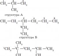
electronic conductivity. In semiconductors, valence electrons "belong" to two neighboring atoms. For example, in a silicon crystal, each pair of neighboring atoms has two "common" electrons. This is shown schematically in Figure 60.1 (only valence electrons are shown here).
The bond between electrons and atoms in semiconductors is weaker than in dielectrics. Therefore, even at room temperature, the thermal energy of some valence electrons is sufficient for them to break away from their pair of atoms, becoming conduction electrons. So in a semiconductor there are negative charge carriers.
The conductivity of a semiconductor due to the movement of free electrons is called electronic.
hole conduction. When a valence electron becomes a conduction electron, it vacates a place in which an uncompensated positive charge arises. This place is called a hole. A hole corresponds to a positive charge, equal in absolute value to the charge of an electron.